Ceramic In Sem Drifting

Clay Platter With Drift Wood Handles By Chinzpotz With Images Ceramic Platters Clay Pottery

The Simplicity Of The Plates And The Use Of Drift Wood Moss For Photo Ceramic Tableware Pottery Ceramic Pottery

Angela De Mott Oh How I Love This El Arte De La Artesania Arte Vasija

Studio Drift S Obsidian Mirror Made From Chemical Waste Chemical Waste Objects Design Mirror

Pin By Emmy On Let S Eat In 2020 Ceramics Ideas Pottery Ceramic Spoons Ceramics

Anthony Stellaccio Ceramic Clay Ceramic Sculpture Clay Sculpture

Large chamber large stage model hitachi s next generation cold field emission sem offers unmatched low voltage imaging and comprehensive analytical microanalysis with the uncompromised performance of cfe.
Ceramic in sem drifting.

White Ceramic Sugar Bowl Pottery Lidded Container Honey Pot Jar Speckled Clay Kitchen Storage Sugar Contai In 2020 Wheel Thrown Pottery Thrown Pottery Beginner Pottery

Ceramic Catalogs Double Click On Above Image To View Full Picture Frascos Decorados Botellas Frascos

Hoonigan Shows Off Four Driver 2016 Formula Drift Team Car Wrap Design Car Ramps Car Culture
Marianne Rosenberg Koppers Slab Ceramics Ceramic Art Sculpture Raku Ceramics

Vase Sotheby S L13211lot75c38en In 2020 Chinese Ceramics Blue And White Vase

Handmade Handdrawn Ceramics 3 051 Vind Ik Leuks 83 Reacties De Kaartjes Kamer De Kaartjes Kamer Op Instagram Ceramic Painting Pottery Painting Pottery

The Z From Tokyo Drift D Find More Sick Cars Like This At Https Www Facebook Com Tuneruniverse Tokyo Dri Carros De Luxo Carros De Cinema Carros Velozes

Personalised Signpost Couple Ceramic Tile Sign Post Ceramics Ceramic Tiles

Drift It S Driftsaturday Again Check The Bestofdrift At Rvinyl S Blog Blog Rvinyl Com Auto

Ceramic Cat Ceramics Projects Clay Crafts Kids Pottery

Radiolarian This Is A Most Beautiful Protozoa Scanning Electron Microscope Science Images Image

Frazier Drift Wood Planter Wood Planters Wood Planters

Round Mango Wood Serving Bowl 33oz Blue Floral Threshold Target Wood Serving Bowl Serving Bowls Mango Wood

Baton De Marche Tete D Animaux En Ceramique Utilitaire Et Decoratif Ceramique Bois Flotte Fait Main Baton De Marche Ceramique Animaux En Ceramique

Image Of Drifter Mug Mok Versieren Porselein Papieren Boten

4 Colors Kawaii Cat Ceramics Bowl K12742 Cute Kitchen Kawaii Cat Cool Things To Buy

Liberate Your Fear Take The Journey By Cathy Broski Ceramic Sculpture Available At Www Artfulhome Com Ceramics Ceramic Artists Sculpture

Films Of Studio Drift Amsterdam Colored Shadow Concrete Art Art And Technology

Builddirect Salerno Porcelain Tile Drift Stone Porcelain Tile Builddirect Stone Collection
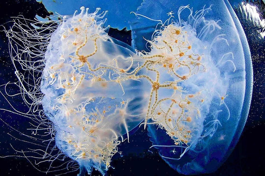
Photograph By Thomaspeschak Jellyfish And Brittlestar Hitchhikers Relatives Of Sea Stars Drifting T Jellyfish National Geographic National Geographic Photos

Pin On Shade Plants Seeds

Set Of 5 Turquoise Bowls Unique Mini Ceramic Bowl Ceramic Etsy In 2020 Turquoise Bowl Raku Pottery Ceramic Gifts

Overstock Com Online Shopping Bedding Furniture Electronics Jewelry Clothing More Red Vases Vase Ceramics Pottery Vase

Round And Blue Contemporary Table Setting Tableware Ceramics
Source : pinterest.com
